The MIPS CPU project represents a comprehensive implementation of a production-quality 32-bit processor compatible with the MIPS1 instruction set architecture. Developed as a collaborative team effort at Imperial College London, this project focused on creating a piece of intellectual property suitable for distribution and integration into various products.
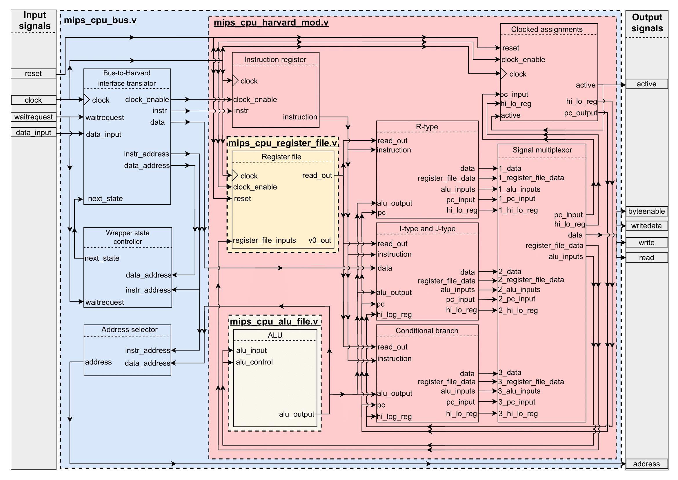
The CPU implements a modified Harvard architecture with a bus-based memory interface, providing flexibility for different memory configurations and peripheral devices. The design supports the complete MIPS1 instruction set as specified in Revision 3.2 of the ISA specification, including arithmetic operations, logical operations, branching, jumping, memory access, and multiplication/division instructions.
Core features include support for 47 distinct instructions covering all major operation categories. Arithmetic instructions handle both signed and unsigned operations with proper overflow handling. The branching logic implements all comparison types including equality, inequality, and magnitude comparisons. Memory operations support byte, half-word, and word access with both aligned and unaligned addressing through the LWL and LWR instructions.
The datapath architecture incorporates a full ALU for arithmetic and logical operations, dedicated multiplication and division units with separate HI and LO registers for storing results, and a comprehensive control unit that generates appropriate signals for each instruction type. The design emphasizes timing optimization and area efficiency, making it suitable for FPGA implementation.
Testing infrastructure represents a critical component of the project, with a comprehensive test suite validating each instruction’s functionality across various edge cases and input combinations. The test bench implements automated verification procedures that can validate any MIPS-compatible CPU implementation, not just the specific design created by the team.
Memory mapping follows standard conventions with execution starting at address 0xBFC00000 after reset, and special handling for address 0x00000000 which triggers CPU halt. The architecture makes no assumptions about peripheral locations, allowing flexible integration into diverse system configurations.
Documentation includes detailed datasheets covering instruction timings, supported features, and integration guidelines. The design has been synthesized and verified on FPGA hardware, demonstrating successful operation across the full instruction set. This project showcases expertise in digital design, verification methodologies, and collaborative hardware development practices.